CIRCUIT PORTFOLIO

From specification.
To physical design.

10 circuit designs developed with AI-assisted workflows, from analog blocks to full-chip integration. Explore layouts, simulation results and technology-specific verification.

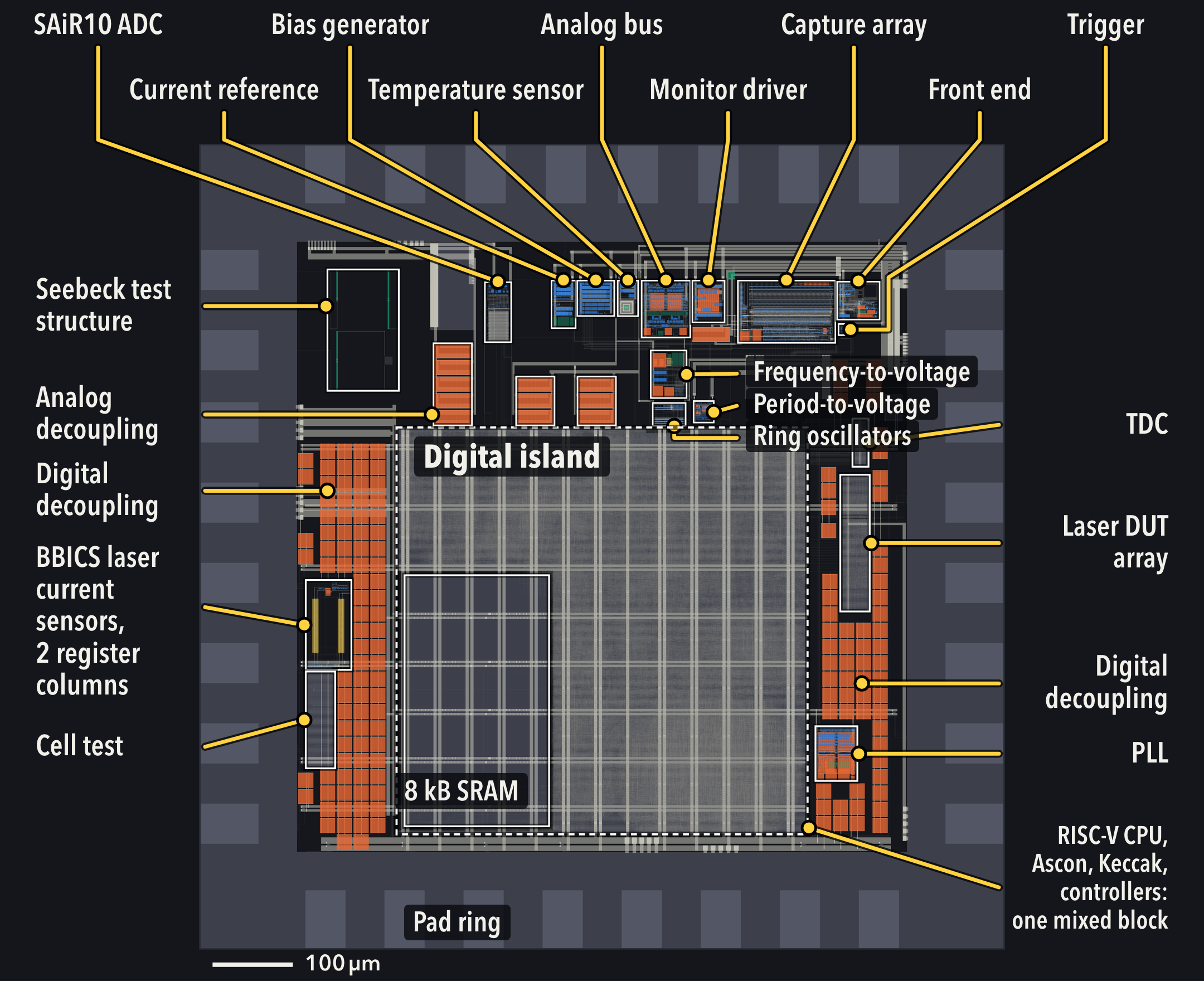
Annotated AiSIC physical layout showing the analog instrumentation, laser test structures, digital island, SRAM and pad ring

FULL-CHIP INTEGRATION

AiSIC mixed-signal test chip

A 65-nm mixed-signal test chip for laser fault-injection research, bringing together analog instrumentation, sensing structures and a RISC-V digital subsystem. Its development combines AI-assisted design and integration with human engineering direction.

65 nm CMOS · 1 × 1 mm die · 21 blocks · 32 pads

Explore this circuit
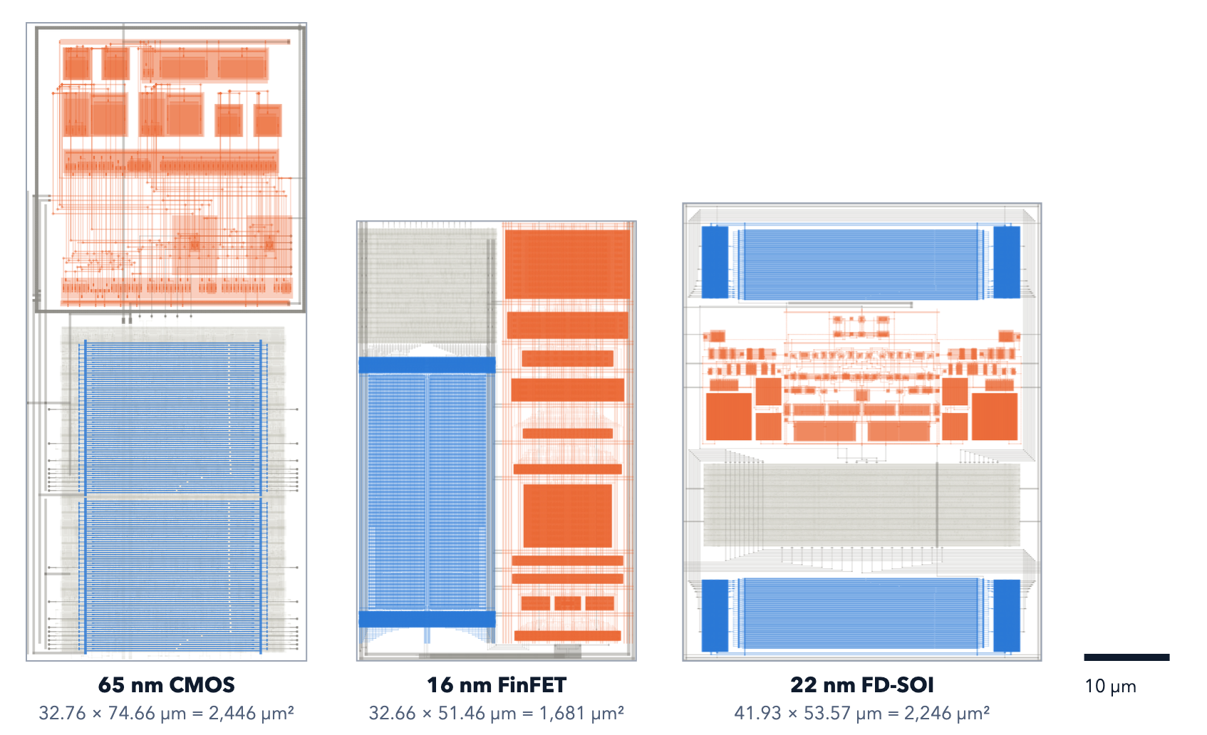
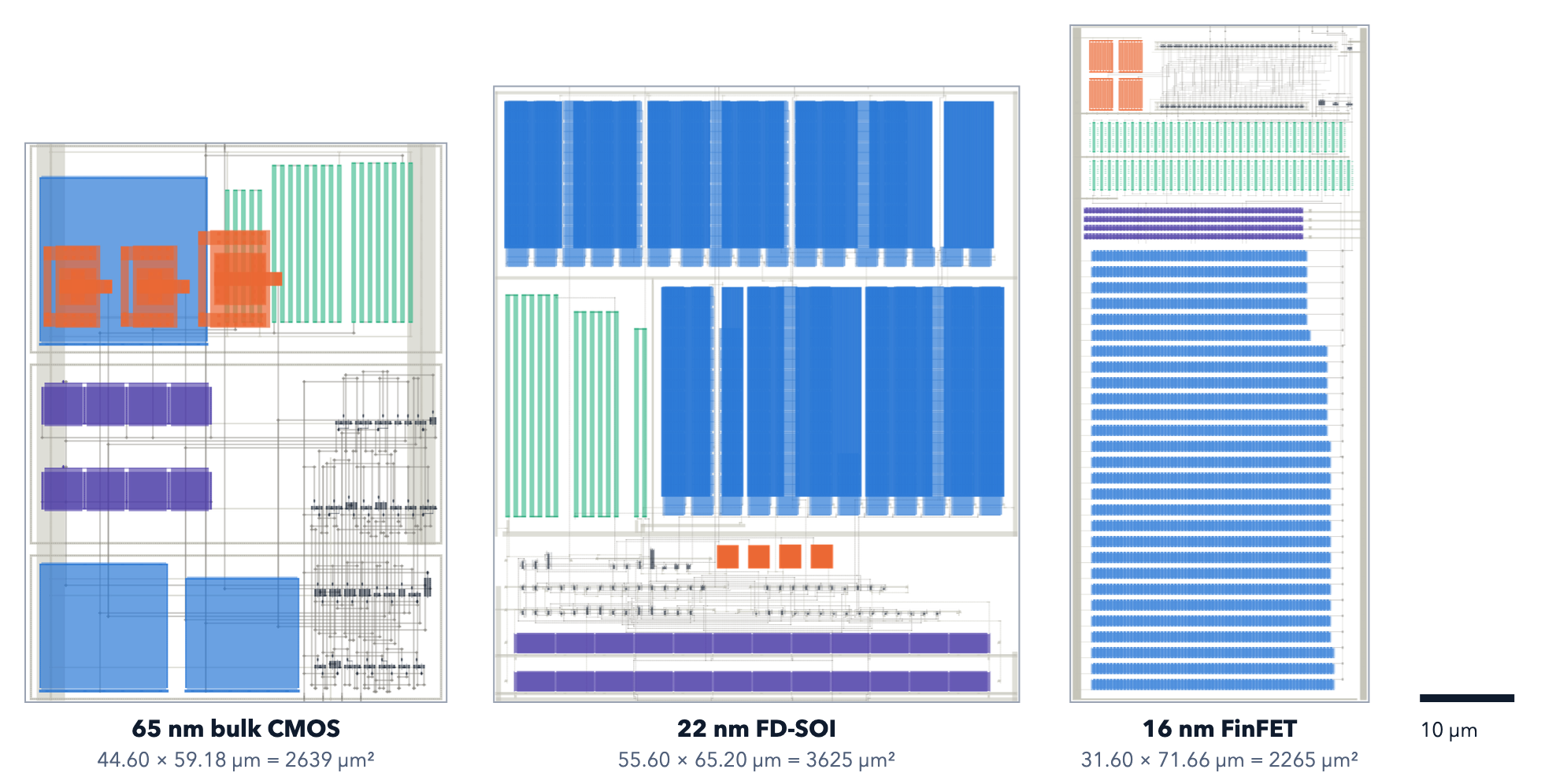
Three SAiR10 ADC layouts shown at one scale

Data conversion

SAiR10 SAR ADC

A 10-bit, 5-MS/s asynchronous SAR ADC taken from a common specification to three technology-specific layouts.

65 nm CMOS · 22 nm FD-SOI · 16 nm FinFET

Explore this circuit
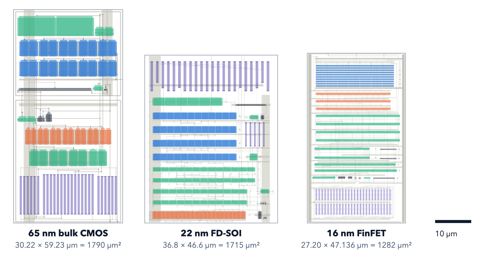
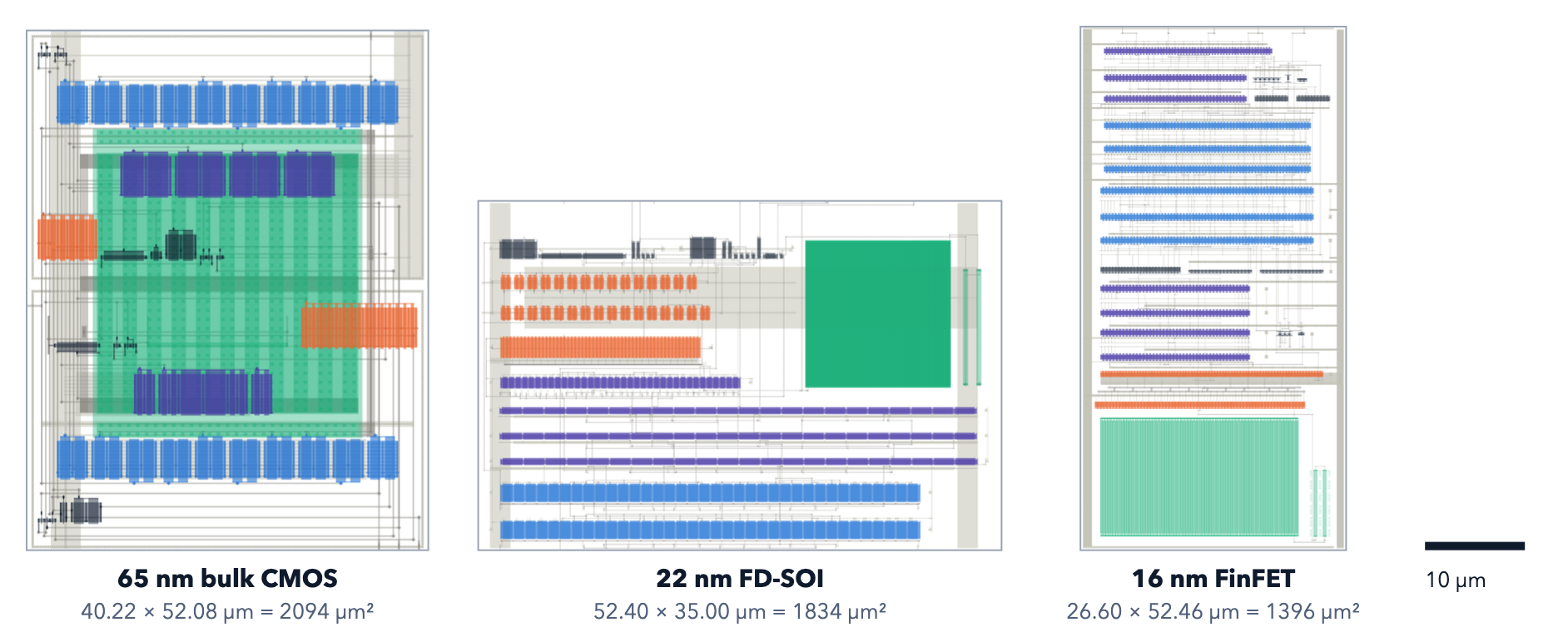
PTAT temperature-sensor layouts in three technologies at one scale

Analog building block

PTAT temperature sensor

A switched-current ΔVBE sensor across bulk CMOS, FD-SOI and FinFET, with signed-off layouts and complete temperature, noise and Monte Carlo characterization.

65 nm CMOS · 22 nm FD-SOI · 16 nm FinFET

Explore this circuit
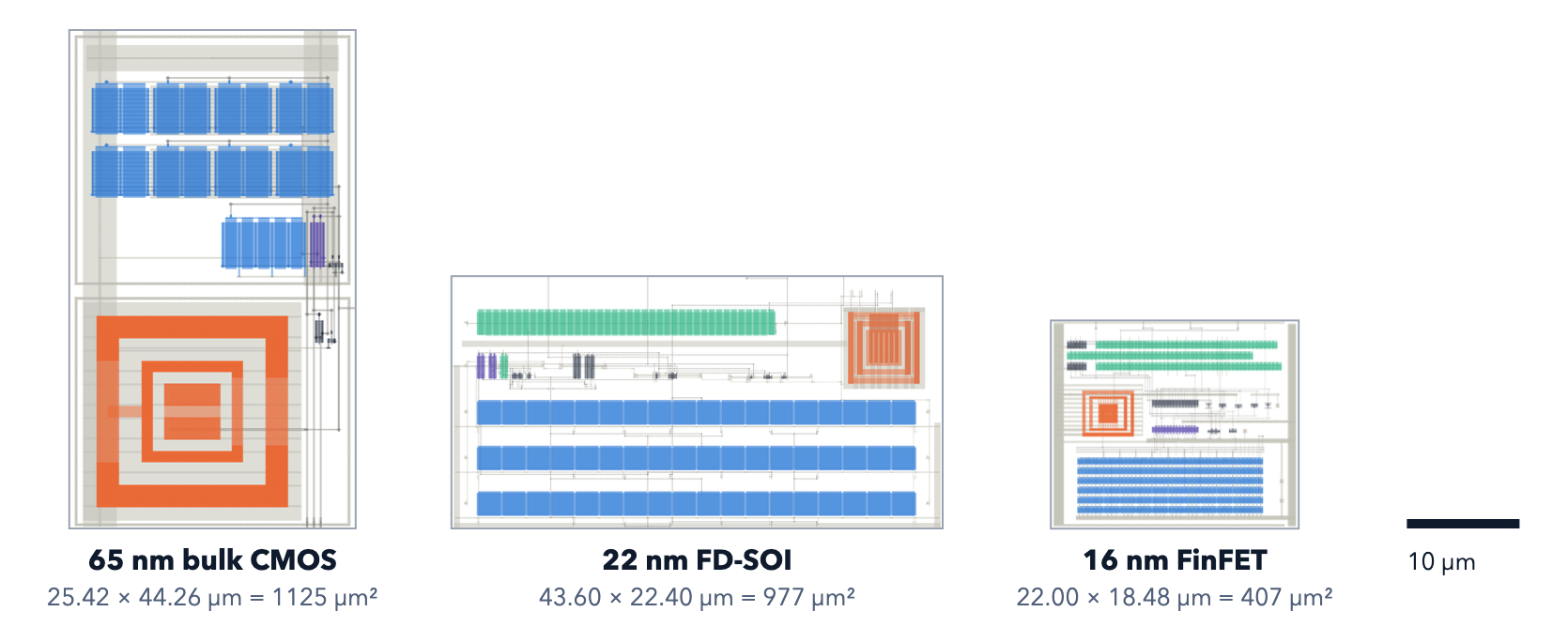
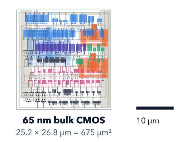
Monitor buffer layouts in 65 nm bulk CMOS, 22 nm FD-SOI and 16 nm FinFET at one scale

Analog building block

Monitor buffer

A rail-to-rail unity-gain amplifier driving the pad, board and scope load. Explore performance tables and 13 characterization figures from retained sign-off data, with technology coverage identified per plot.

65 nm CMOS · 22 nm FD-SOI · 16 nm FinFET

Explore this circuit
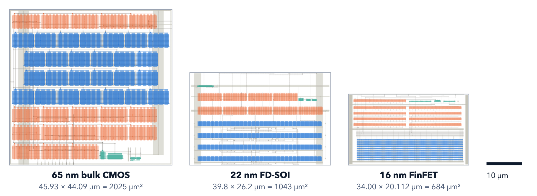
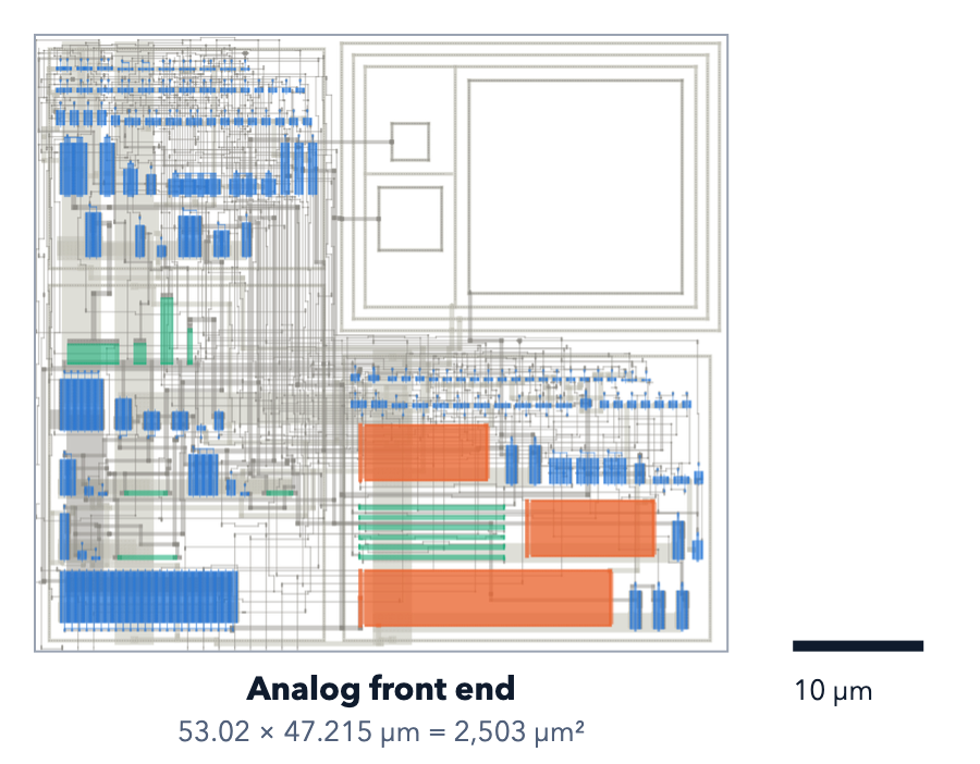
Analog front end layout in 65 nm bulk CMOS with a 10 µm scale bar

Laser-capture front end

Analog front end

Three sensing paths with programmable transimpedance gain, matched response and on-chip electrical calibration.

65 nm bulk CMOS · Layout and technical results

Explore this circuit

Showing all 10 circuits.

These designs include physical layouts and simulation results. Each page states its verification status, operating conditions and remaining checks; results are not measured-silicon data.

LET’S MAKE IT CONCRETE

Bring Trame into
your design team.

Discuss the circuits, tools and workflows your team needs to support.

Discuss your project