
What it does
65 nm bulk CMOS · AiSIC SoC
The front end of the laser-capture path. Three sense junctions of different size (n-well in the p-type substrate, 3.5, 5.5 and 17 µm squares) sit under the same laser spot. One of them is selected, and its photocurrent is turned into a voltage on the sampling bus, which the capture array samples. The three paths are built to respond identically, so that the photocurrent profile can be compared against junction size. An electrical test pulse injects a current step with the photocurrent's polarity into the selected junction, so that each path's step response can be measured on chip.
How it works
65 nm bulk CMOS · AiSIC SoC
Each path is a regulated common-gate stage: a transistor takes the photocurrent at the junction and passes it to a shared load node, and a booster amplifier drives its gate. Every path runs at the same bias current (120 µA) and feeds the same gain leg, so gain and dark level are the same for every path by construction; only the input transistor and the booster scale with the junction, which evens out the bandwidth. Three gains (250 Ω, 1 kΩ and 4 kΩ transimpedance) are selected by switched resistor loads. An unselected junction is held reverse-biased by a dump transistor that also sinks its photocurrent. A source follower (2.4 mA) drives the sampling bus and the hold cells of the capture array.
Two loads are evaluated: one hold cell (equivalent-time mode, one sample per repeated laser shot) and the 61 hold cells of the single-shot mode.
The layout, at one scale
65 nm bulk CMOS · AiSIC SoC
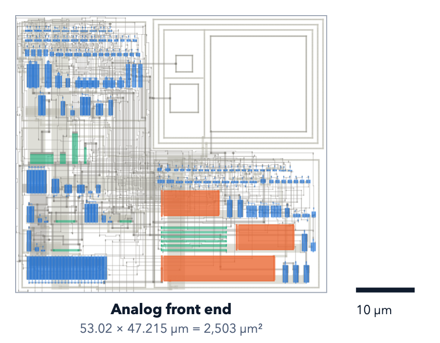
Area (drawn macro outline): Analog front end 53.02 × 47.215 µm = 2,503 µm².
Key numbers
65 nm bulk CMOS · AiSIC SoC
Post-layout simulation with extracted parasitics, not silicon. 65 nm bulk CMOS, the released layout. Corners: tt typical, ss / ff slow / fast, sf / fs mixed; temperatures 0 to 85 °C.
| Measure | Value | Specification | Basis |
|---|---|---|---|
| Rise time 10–90 %, gain 250 Ω, one-cell load | 34.9–73.3 ps | ≤ 100 ps (target) | post-layout, 5 corners |
| Rise time 10–90 %, gain 250 Ω, 61-cell load | 59.0–116.8 ps | ≤ 100 ps target; owner-accepted value 124.9 ps | post-layout, 45 points |
| Step overshoot, 61-cell load | 2.45 % worst | ≤ 5 % | post-layout, 45 points |
| Gain matching of the three paths, full-scale steps | 1.00 % (250 Ω), 0.35 % (1 kΩ), 0.17 % (4 kΩ) | ≤ 2 % | post-layout, 45 points |
| Gain matching of the three paths, small signal, Monte Carlo | 0.166 % (1σ, 200 runs) | ≤ 1 % (1σ) | post-layout Monte Carlo of the first layout of the same circuit |
| Rise-time spread between the three paths, 61-cell load | 13.1 % (250 Ω), 11.7 % (1 kΩ), 14.7 % (4 kΩ) | ≤ 20 % | post-layout, 45 points |
| Recovery from a 5× / 20× full-scale overload, to 1 % | 5.06 / 5.86 ns | ≤ 10 ns | post-layout, 3 points |
| Dark level settled to 1 mV after a control change (enable / select / gain) | 353.1 / 162.6 / 274.3 ns | ≤ 2 µs | post-layout, 3 points |
| Signal from an unselected junction (300 µA into it) | 0.47 mV | ≤ 1 mV at the held node | post-layout, 3 points |
| Power while armed | 3.95–4.51 mW typical; up to 5.51 mW (ff, 85 °C, 1.26 V) | about 5 mW with the capture array (target) | post-layout, 45 points |
| Gate-oxide overvoltage (above 1.32 V for 0.1 ns or more) | 0 events | 0 events | post-layout, 15 top-supply points, with the control-sequence rule below |
| Current-density margin, worst wire | 1.023 | ≥ 1 | post-layout, 2430 operating points |
| Supply drop to a current-carrying device (supply / ground) | 7.93 / 7.35 mV | ≤ 1 % of the supply (11.4 mV) | post-layout, 2430 operating points |
Use rules
65 nm bulk CMOS · AiSIC SoC
Control-sequence rule (built into the chip's control logic): the test-pulse enable and its amplitude bits never switch in the same clock cycle, and the control edges at the front end's inputs are 0.3 ns or slower. With this rule the gate-oxide check finds no event at any of the 15 top-supply points.