
One monitor buffer. Three technologies.
Unity-gain buffering from the on-chip monitor to the pad, board and oscilloscope load.
Copies an internal analog voltage to a pad so a scope can observe the signal without loading the circuit that produces it.
Characterization release: 13 figures replotted from retained sign-off data. No new simulations were run. Each figure identifies the available technologies.
Performance tables → Explore the curves →
| Measure | 65 nm bulk CMOS | 22 nm FD-SOI | 16 nm FinFET |
|---|---|---|---|
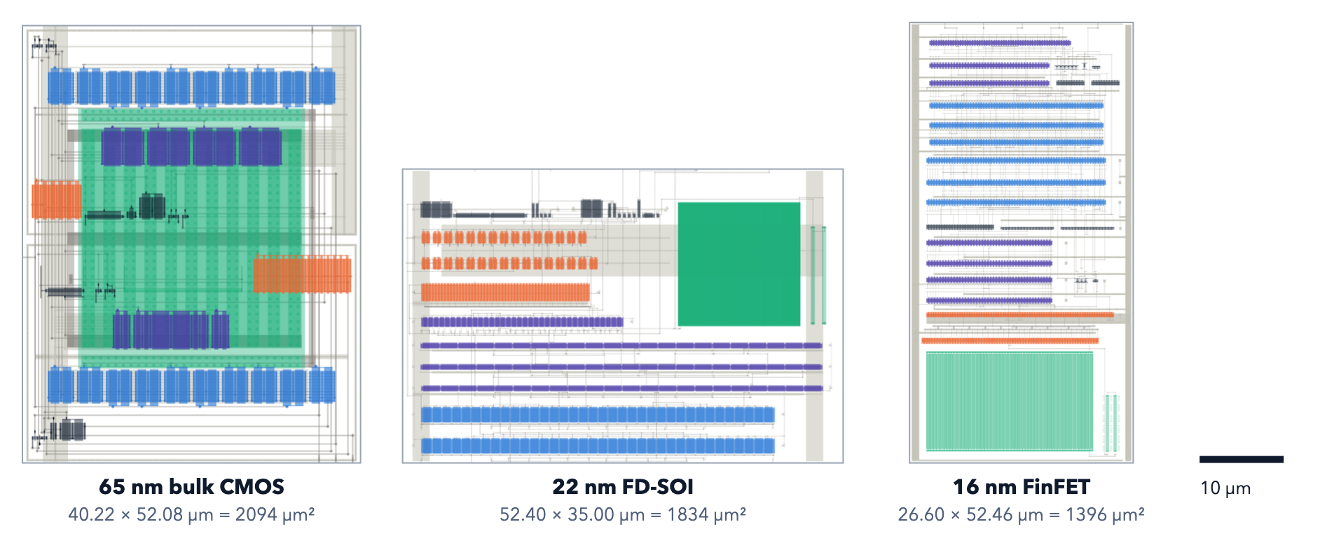
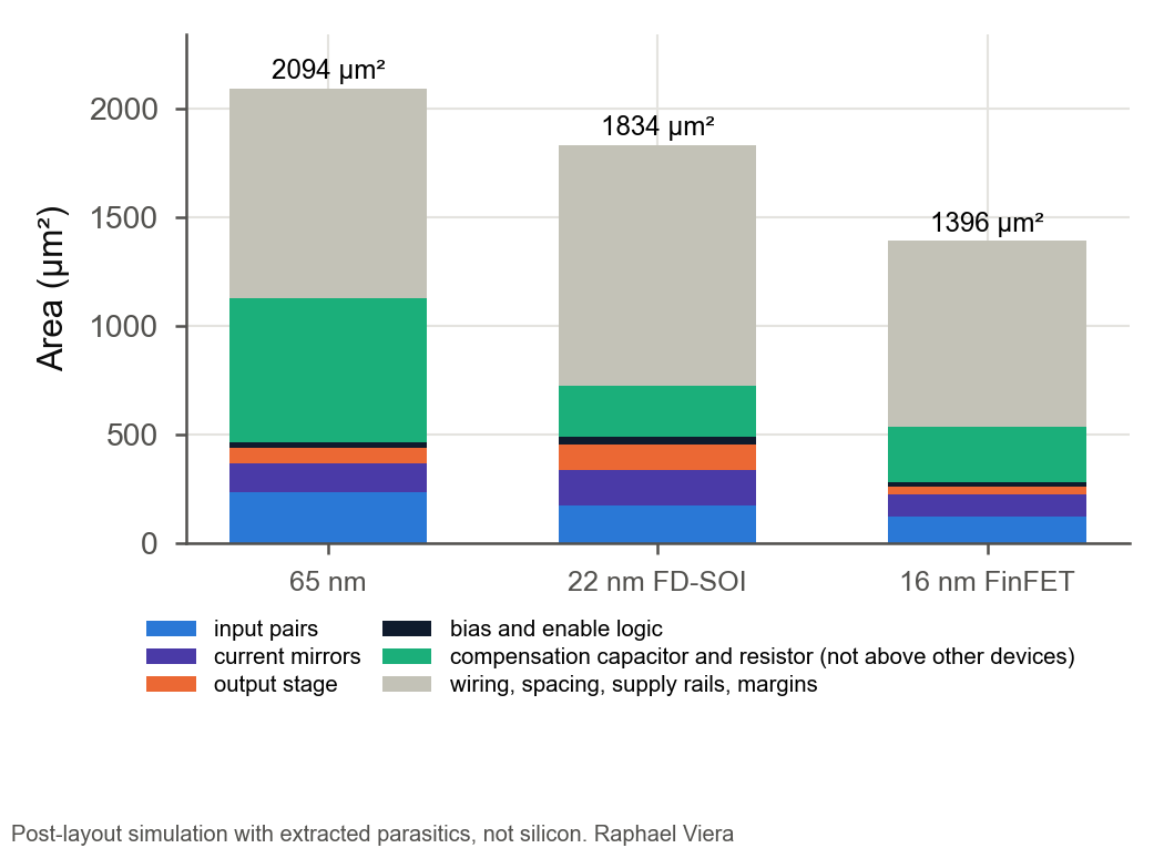
| Drawn macro area | 2,094 µm² | 1,834 µm² | 1,396 µm² |
| Macro dimensions | 40.22 × 52.08 µm | 52.40 × 35.00 µm | 26.60 × 52.46 µm |
Post-layout simulation with extracted parasitics, not silicon measurements.
From the monitor to the scope
A rail-to-rail unity-gain amplifier, with a class-A output stage and Miller compensation.
Sense
Two complementary input pairs provide the rail-to-rail input structure.
Combine
Both input pairs feed one folded summing mirror.
Drive
A class-A output stage drives the pad. A 1.4-pF Miller capacitor keeps the amplifier stable into the pad, board and scope load.
Human-directed implementation
AI agents performed the design, layout and verification under human direction, with less than one hour of human hands-on time for the work presented here.
The implementations span 65-nm bulk CMOS, 22-nm FD-SOI and 16-nm FinFET. The evidence is post-layout simulation with extracted parasitics, not measured silicon.
The layouts, at one scale
65-nm bulk CMOS · 22-nm FD-SOI · 16-nm FinFET
Performance
Post-layout simulation with extracted parasitics · 65 nm CMOS, 22 nm FD-SOI and 16 nm FinFET
| 65 nm bulk CMOS | 22 nm FD-SOI | 16 nm FinFET | specification | |
|---|---|---|---|---|
| Area | 2094 µm² (40.22 × 52.08 µm) | 1834 µm² (52.40 × 35.00 µm) | 1396 µm² (26.60 × 52.46 µm) | drawn macro outline |
| Supply | 1.2 V | 0.8 V | 0.8 V | |
| Input offset, 1σ ¹ | 1.69 mV | 1.13 mV (worst-case model 2.10 mV) | 1.14 mV | ≤ 2 mV |
| Noise at 1 MHz ² | 36.2 nV/√Hz | 45.2 nV/√Hz | 47.2 nV/√Hz | ≤ 50 nV/√Hz |
| Settling to ±0.25 mV ² | 976 ns | 982 ns | 741 ns | ≤ 1 µs |
| Supply rejection at DC ² | 65 dB | 68 dB | 80 dB | ≥ 50 dB |
| Power, typical ³ | 80.2 µW | 50.5 µW | 50.6 µW | ≤ 100 µW |
¹ 1σ over 200 Monte Carlo chips at the worst input level; 22 nm on the best-case matching model, the design basis. ² Worst corner simulated. ³ 65 nm: the supply-power increase when the buffer is enabled; 22 and 16 nm: including its own 10 µA bias branch.
Load: the pad, the board and a scope input, 26.65 pF in parallel with 1 MΩ; stable from 1.65 to 41.65 pF. Input range: 0.15 V from each rail. In use, every reading is offset-calibrated.
Characterization scope
Retained sign-off data · No new simulations were run for this plot release.
Typical conditions are tt, 27 °C and nominal supply unless stated otherwise. Technology coverage and simulated points differ by figure; each plot identifies its available evidence.
| Quantity | 65 nm CMOS | 22 nm FD-SOI | 16 nm FinFET | Basis |
|---|---|---|---|---|
| Area (drawn macro) | 2094 µm² | 1834 µm² | 1396 µm² | drawn layout |
| Supply | 1.2 V ±5 % | 0.8 V ±5 % | 0.8 V ±5 % | design |
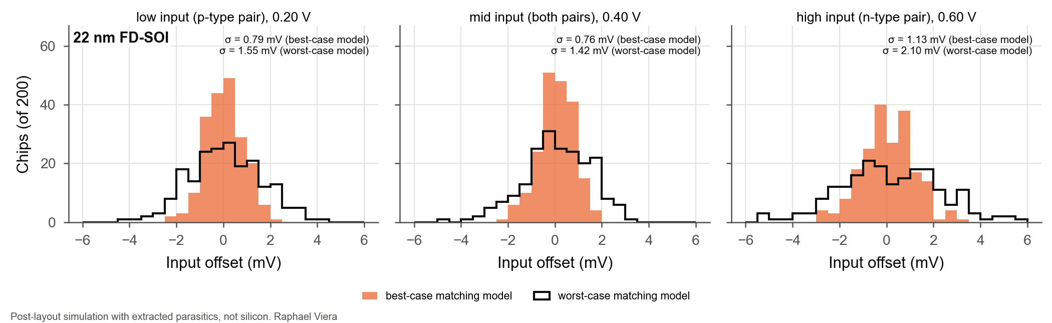
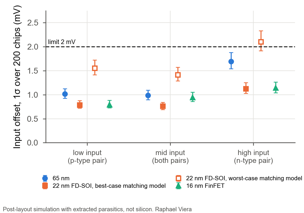
| Input offset, 1σ over 200 chips, at low / mid / high input | 1.01 / 0.99 / 1.69 mV | 0.79 / 0.76 / 1.13 mV (worst-case matching model 1.55 / 1.42 / 2.10 mV) | 0.80 / 0.95 / 1.14 mV | post-layout |
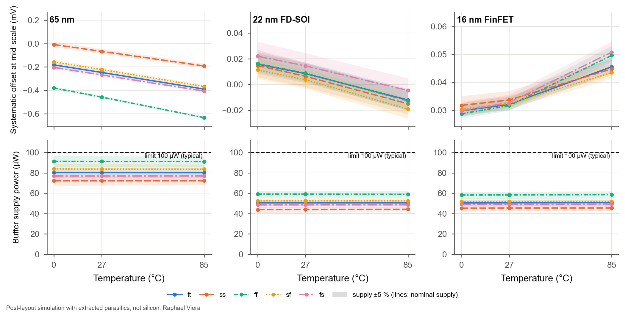
| Systematic offset at mid-scale, 45 points | -0.64 to 0.02 mV | -0.026 to 0.033 mV | 0.027 to 0.055 mV | post-layout |
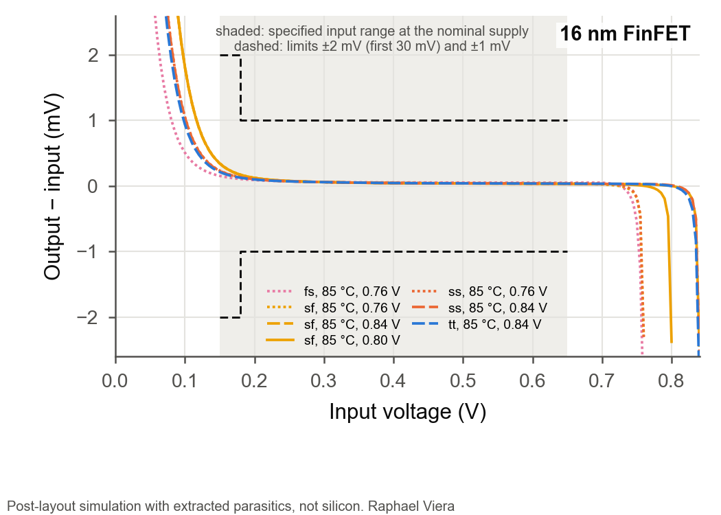
| DC error over the specified input range: first 30 mV / above (largest of the simulated points) | - | 1.85 / 0.84 mV (45 points) | 0.30 / 0.13 mV (7 points) | post-layout |
| Input range with the DC error within ±1 mV of its mid-scale value (worst ends over 45 points) | 0.10 V to supply − 0.12 V | 0.175 V to supply − 0.010 V | 0.120 V to supply − 0.010 V | post-layout |
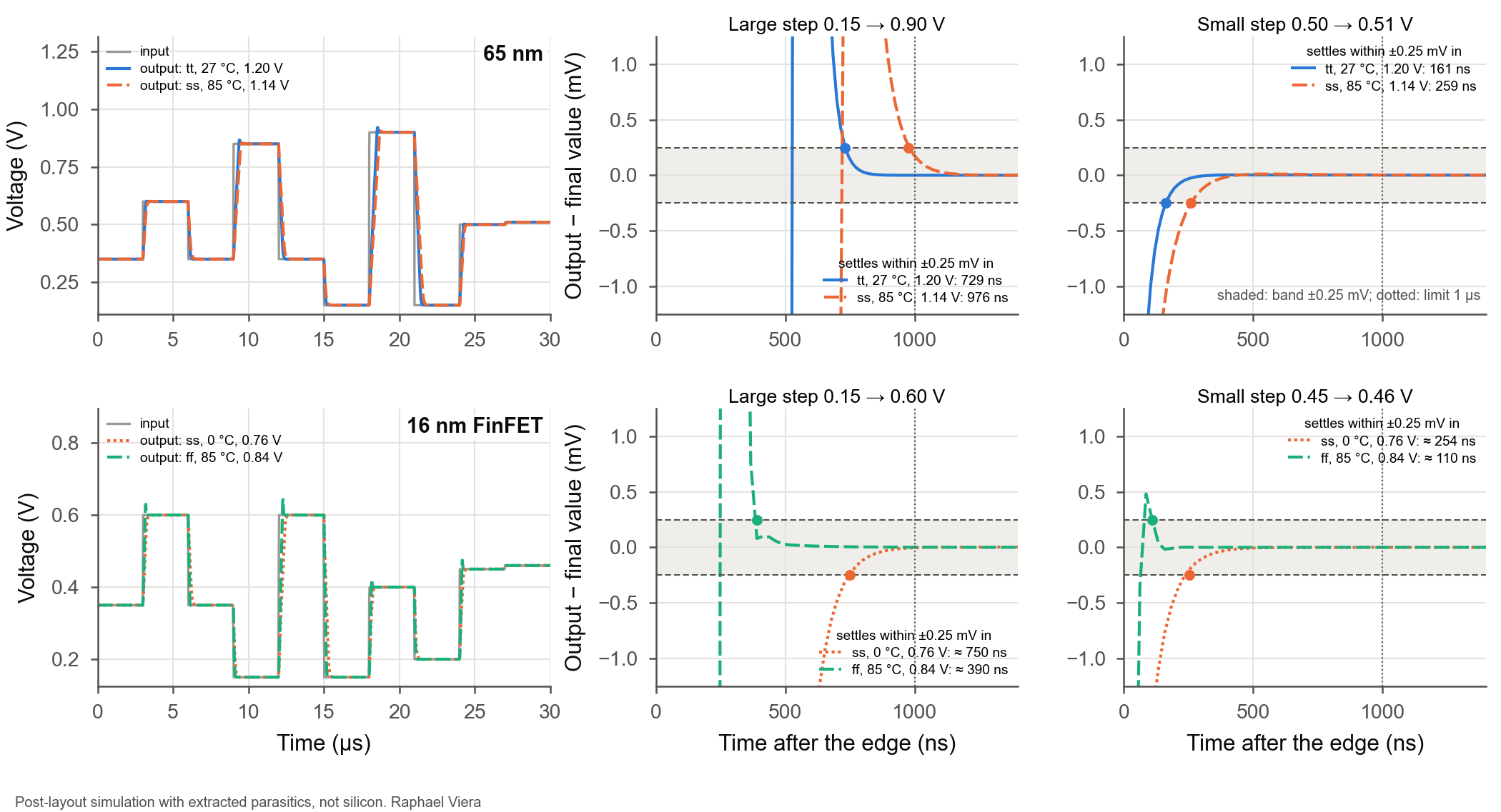
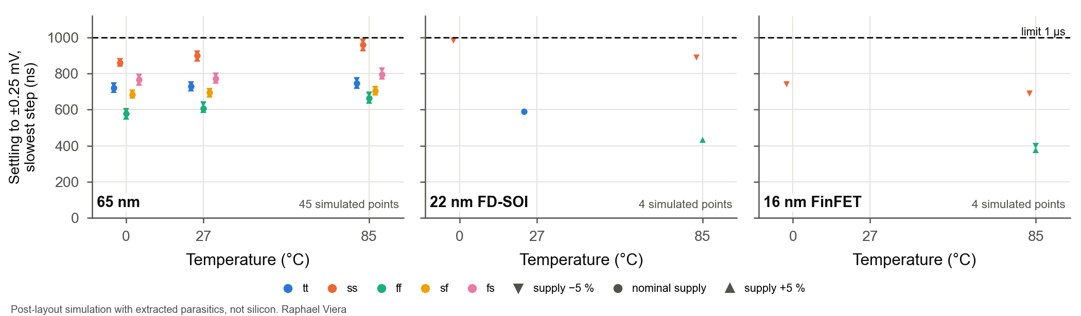
| Settling to ±0.25 mV / ±1 mV, slowest step, slowest simulated point | 976 / 896 ns (45 points) | 982 / 857 ns (4 points) | 741 / 646 ns (4 points) | post-layout |
| Settling to ±0.25 mV at the typical corner | 729 ns | 590 ns | - | post-layout |
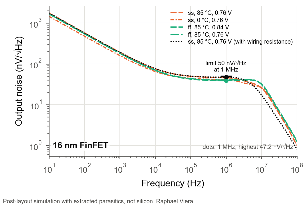
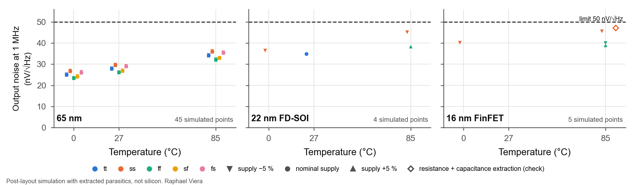
| Output noise at 1 MHz: highest simulated point / typical corner | 36.2 / 28.0 nV/√Hz | 45.2 / 34.9 nV/√Hz | 47.2 nV/√Hz | post-layout |
| Output noise integrated from 10 Hz to 100 MHz | 81 to 98 µV rms | 106 to 119 µV rms | 120 to 149 µV rms | post-layout |
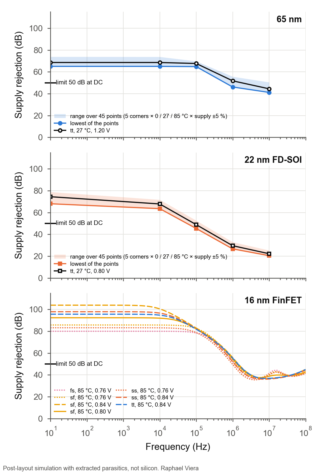
| Supply rejection at DC / 1 MHz, lowest simulated point | 65.0 / 46.2 dB | 68.0 / 26.7 dB | 80.0 / 49.6 dB (7 points) | post-layout |
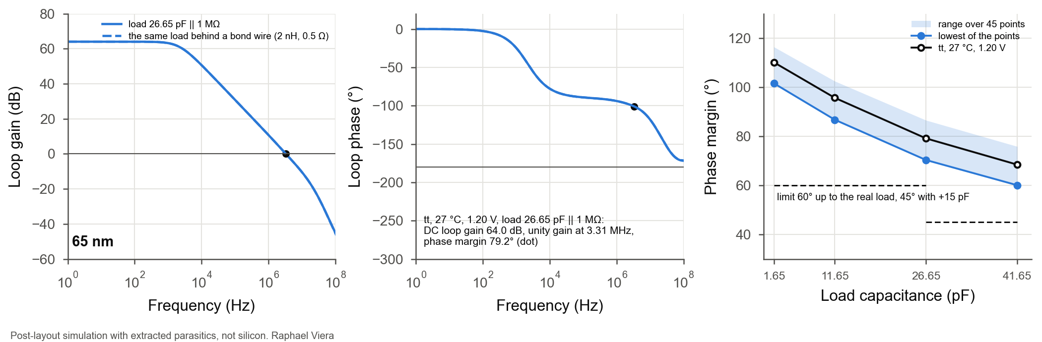
| Phase margin into the real load: lowest of 45 points / typical corner | 70.4° / 79.2° | - (schematic: 76.2° lowest) | - (schematic: 70.7° lowest) | post-layout |
| Phase margin at 1.65 pF / 41.65 pF, lowest of 45 points | 101.6° / 60.1° | - (schematic: 101.3° / 66.5°) | - (schematic: 97.7° / 61.1°) | post-layout |
| Unity-gain frequency of the loop, 45 points | 2.14 to 4.64 MHz | - | - | post-layout |
| Supply power of the buffer: typical corner / range over 45 points | 80.2 µW / 67.5 to 96.7 µW | 50.5 µW / 40.8 to 62.4 µW | 50.6 µW / 42.1 to 61.8 µW | post-layout |
| Output resistance at DC / load regulation for ±10 µA (largest) | 34.5 Ω / 0.37 mV | 2.2 Ω / 0.025 mV | 0.9 Ω / 0.010 mV | post-layout |
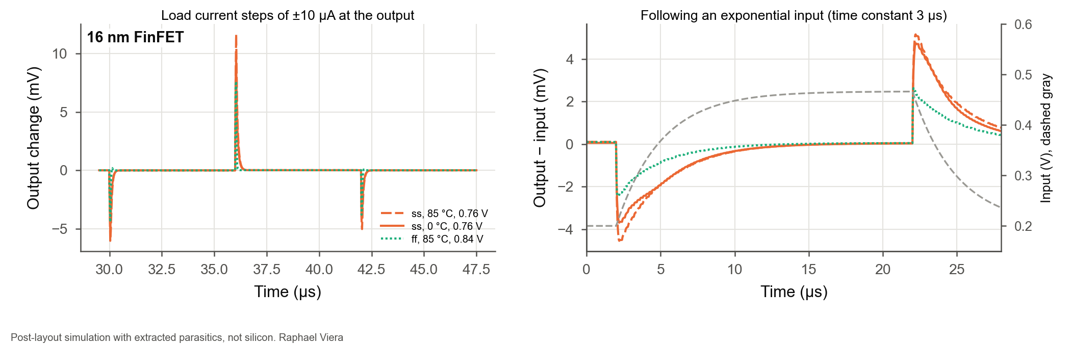
| Load step of ±10 µA: peak / recovery to 0.1 mV (largest) | not simulated | 14.4 mV / 477 ns | 11.9 mV / 380 ns | post-layout |
A dash means a post-layout value is not available in this release. Schematic values are identified separately; “not simulated” is retained where stated. Missing curves do not imply a measured result or a new simulation.
Post-layout simulation with extracted parasitics, not silicon measurements.
Step response
65 nm bulk CMOS · 16 nm FinFET · Retained sign-off data
Settling across PVT
65 nm bulk CMOS · 22 nm FD-SOI · 16 nm FinFET · Retained sign-off data
DC error vs input
16 nm FinFET only · Retained sign-off data
Noise spectrum
16 nm FinFET only · Retained sign-off data
Noise at 1 MHz
65 nm bulk CMOS · 22 nm FD-SOI · 16 nm FinFET · Retained sign-off data
Supply rejection
65 nm bulk CMOS · 22 nm FD-SOI · 16 nm FinFET · Retained sign-off data
Loop gain & stability
65 nm bulk CMOS only · Retained sign-off data
Offset distribution
22 nm FD-SOI only · Retained sign-off data
Offset vs input level
65 nm bulk CMOS · 22 nm FD-SOI · 16 nm FinFET · Retained sign-off data
Offset & power vs temperature
65 nm bulk CMOS · 22 nm FD-SOI · 16 nm FinFET · Retained sign-off data
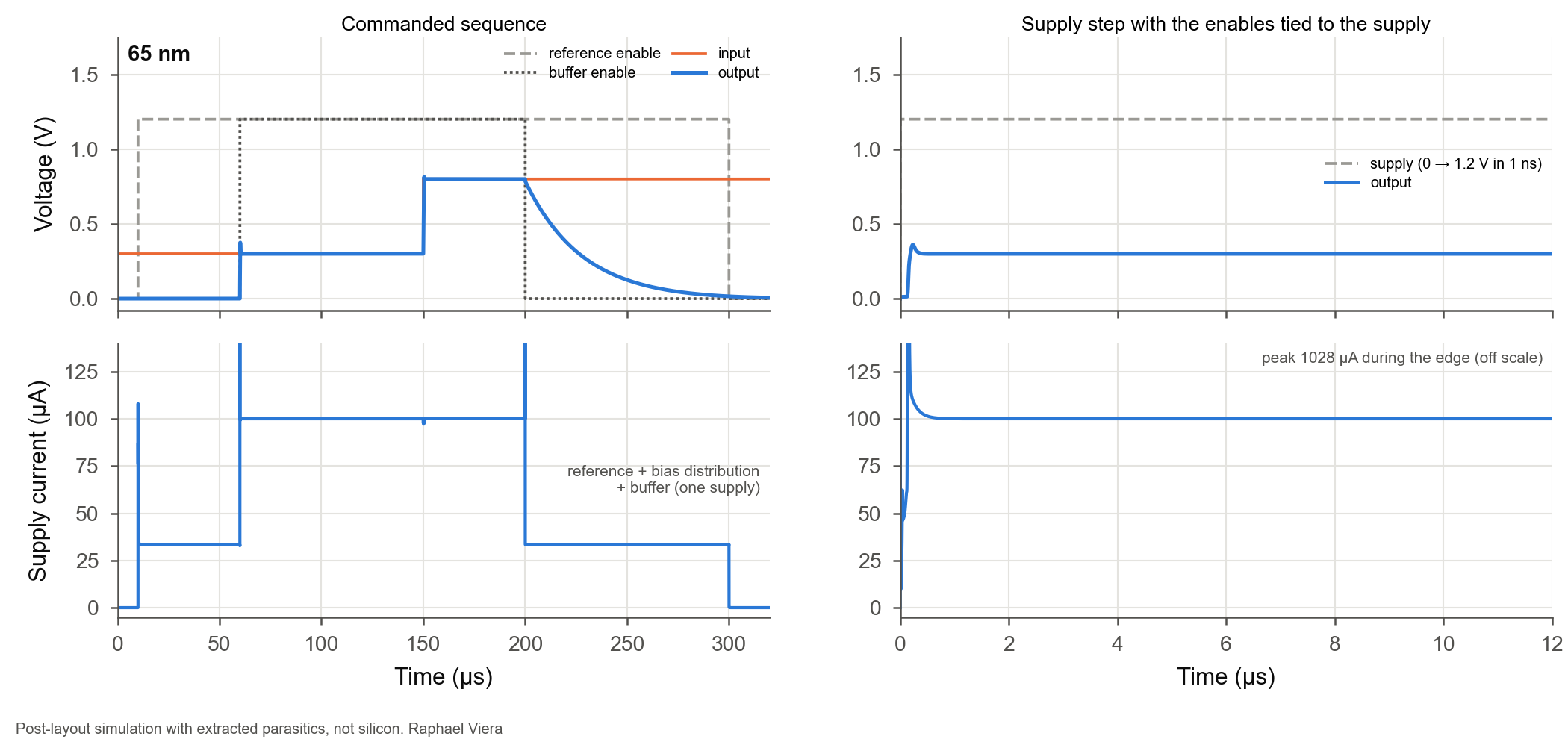
Enable & start-up
65 nm bulk CMOS only · Retained sign-off data
Load step & tracking
16 nm FinFET only · Retained sign-off data
Area by function
65 nm bulk CMOS · 22 nm FD-SOI · 16 nm FinFET · Retained sign-off data
Literature comparison
Reference values supplied with this release · Check the basis and test conditions before comparing.
This work is post-layout simulation, not measured silicon. The references include silicon, post-layout and other simulation results, identified in the Basis column. Loads, supply, speed definitions and area boundaries differ; this is not a like-for-like performance ranking. n/s means not stated in the supplied comparison.
| # | Reference | Year | Technology | Supply | Load | Speed, as stated | Quiescent current or power | Offset | Noise | Area | Basis | DOI |
|---|---|---|---|---|---|---|---|---|---|---|---|---|
| [1] | R. Hogervorst, J. P. Tero, R. G. H. Eschauzier, J. H. Huijsing, IEEE J. Solid-State Circuits 29(12), 1505-1513 | 1994 | n/s | 3 V | 10 pF | unity-gain frequency 2.6 MHz (Miller), 6.4 MHz (cascoded Miller) | 4 MHz/mW and 11 MHz/mW (bandwidth per supply power) | n/s | n/s | 0.04 mm² | silicon | 10.1109/4.340424 |
| [2] | K.-J. de Langen, J. H. Huijsing, IEEE J. Solid-State Circuits 33(10), 1482-1496 | 1998 | 1.6 µm CMOS | ≥ 1.8 V (rail-to-rail input version ≥ 2.5 V) | 5 pF (gain measured into 10 kΩ) | unity-gain frequency 4 MHz, phase margin 67° | n/s | n/s | 38 nV/√Hz at 100 kHz | 0.08 mm² | silicon | 10.1109/4.720394 |
| [3] | J. M. Carrillo, G. Torelli, R. Pérez-Aloe, J. F. Duque-Carrillo, IEEE J. Solid-State Circuits 42(3), 508-517 | 2007 | 0.35 µm CMOS | 1 V | 17 pF in parallel with 1 MΩ | closed-loop unity-gain bandwidth > 8 MHz | n/s | n/s | n/s | n/s | silicon | 10.1109/JSSC.2006.891717 |
| [4] | C.-W. Lu, IEEE J. Solid-State Circuits 39(11), 1938-1947 | 2004 | 0.35 µm CMOS | 3.3 V | 600 pF | settling 2.7 µs rising, 2.9 µs falling (3.3 V swing) | 7 µA static | n/s | n/s | 46.5 × 57 µm² active | silicon | 10.1109/JSSC.2004.835821 |
| [5] | C.-W. Lu, K.-J. Hsu, IEEE J. Solid-State Circuits 39(8), 1313-1320 | 2004 | 0.35 µm CMOS | n/s | 680 pF | settling ≤ 1.2 µs rising, ≤ 1.4 µs falling | 4.7 µA and 4.2 µA static (the two buffers) | n/s | n/s | n/s | silicon | 10.1109/JSSC.2004.831475 |
| [6] | C.-W. Lu, IEEE J. Solid-State Circuits 44(2), 525-537 | 2009 | 0.35 µm CMOS | 5 V | 140 pF behind 3.4 kΩ | settling 3 µs (5 V swing) | 7.5 µA static | 0.48 mV with the cancellation | n/s | n/s | silicon | 10.1109/JSSC.2008.2010995 |
| [7] | A. D. Grasso, G. Palumbo, S. Pennisi, IEEE Trans. Circuits Syst. II 65(12), 1879-1883 | 2018 | 0.35 µm CMOS | 3 V | 1 nF | settling 1.11 µs (full swing) | 1.6 µA | n/s | n/s | 5562 µm² | silicon | 10.1109/TCSII.2018.2817261 |
| [8] | M. Yıldız, S. Minaei, E. Arslan, J. Circuits Syst. Comput. 20(7), 1277-1286 | 2011 | 0.35 µm CMOS | 3.3 V | 600 pF | average settling 0.85 µs (full swing) | 3 µA | n/s | n/s | n/s | post-layout simulation | 10.1142/S0218126611007888 |
| [9] | E. Arslan, M. Yıldız, S. Minaei, Int. J. Electron. 102(6), 982-992 | 2015 | 0.35 µm CMOS | 3.3 V | 1 nF | n/s ("small settling time") | 1.6 µA | n/s | n/s | n/s | post-layout simulation | 10.1080/00207217.2014.947637 |
| [10] | Y. Huang, C. Luo, T. Lu, Y. Zhang, et al., IEICE Electron. Express 18(12), 20210183 | 2021 | 0.18 µm CMOS | 1.4 V | 10 pF | slew rate +36 / −33.8 V/µs | 55.7 µW static | n/s | n/s | n/s | simulation | 10.1587/elex.18.20210183 |
| this work | monitor buffer, 65 nm CMOS: rail-to-rail unity-gain buffer, class-A output, Miller compensation | 2026 | 65 nm CMOS | 1.2 V | 26.65 pF in parallel with 1 MΩ | settling to ±0.25 mV ≤ 976 ns (0.75 V step, slowest of 45 simulated points) | 80.2 µW (typical corner) | 1.69 mV (1σ, 200 chips, worst input level) | ≤ 36.2 nV/√Hz at 1 MHz | 2094 µm² | post-layout simulation | - |
| this work | monitor buffer, 22 nm FD-SOI: rail-to-rail unity-gain buffer, class-A output, Miller compensation | 2026 | 22 nm FD-SOI | 0.8 V | 26.65 pF in parallel with 1 MΩ | settling to ±0.25 mV ≤ 982 ns (0.45 V step, slowest of 4 simulated points) | 50.5 µW (typical corner) | 1.13 mV (1σ, 200 chips, worst input level) | ≤ 45.2 nV/√Hz at 1 MHz | 1834 µm² | post-layout simulation | - |
| this work | monitor buffer, 16 nm FinFET: rail-to-rail unity-gain buffer, class-A output, Miller compensation | 2026 | 16 nm FinFET | 0.8 V | 26.65 pF in parallel with 1 MΩ | settling to ±0.25 mV ≤ 741 ns (0.45 V step, slowest of 4 simulated points) | 50.6 µW (typical corner) | 1.14 mV (1σ, 200 chips, worst input level) | ≤ 47.2 nV/√Hz at 1 MHz | 1396 µm² | post-layout simulation | - |