Overview
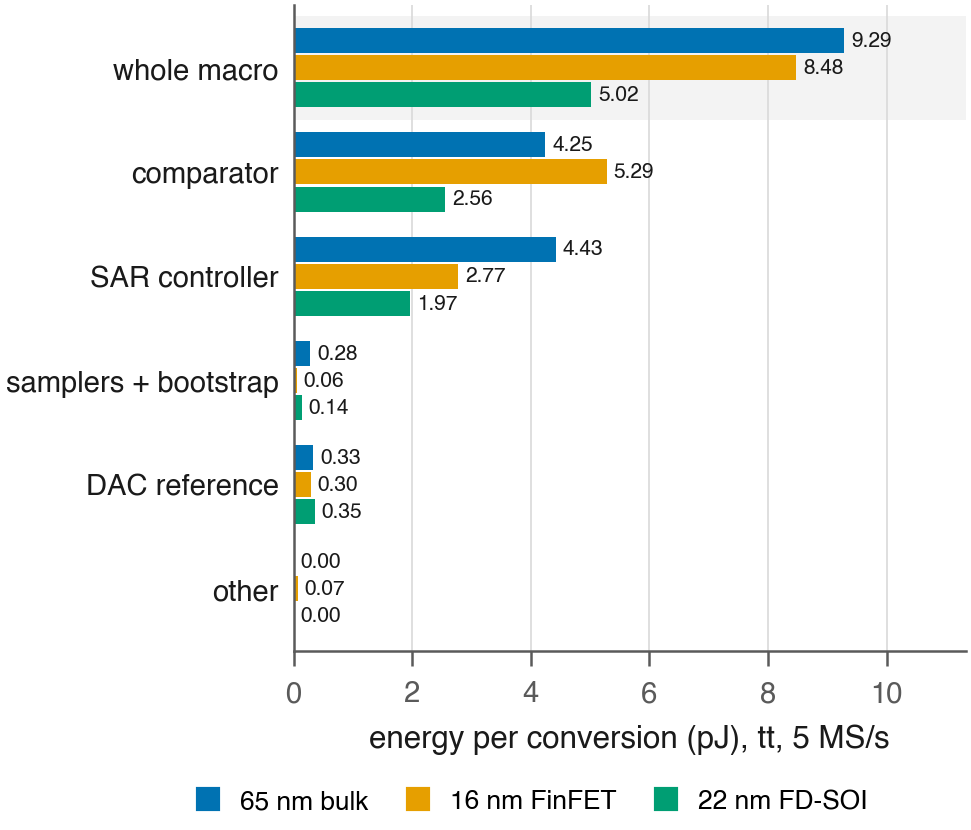
The delivered macros in one comparison.
Physical verification
DRC, LVS and antenna checks; technology-specific scope is recorded in the sign-off details.
Electrical verification
PVT, Monte Carlo, linearity, conversion timing and start-up.
Extracted-layout results
Post-layout simulation across 65-nm bulk CMOS, 16-nm FinFET and 22-nm FD-SOI.
| Measure | 65-nm bulk | 16-nm FinFET | 22-nm FD-SOI |
|---|---|---|---|
| Supply | 1.2 V | 0.8 V | 0.8 V |
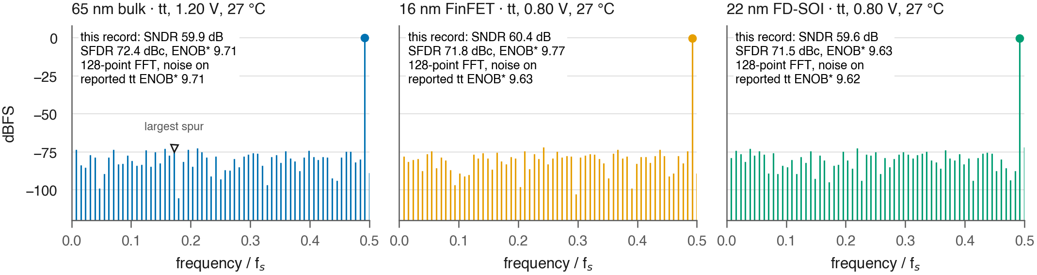
| Typical ENOB* | 9.71 bit | 9.63 bit | 9.62 bit |
| Typical SNDR* | 60.2 dB | 59.8 dB | 59.6 dB |
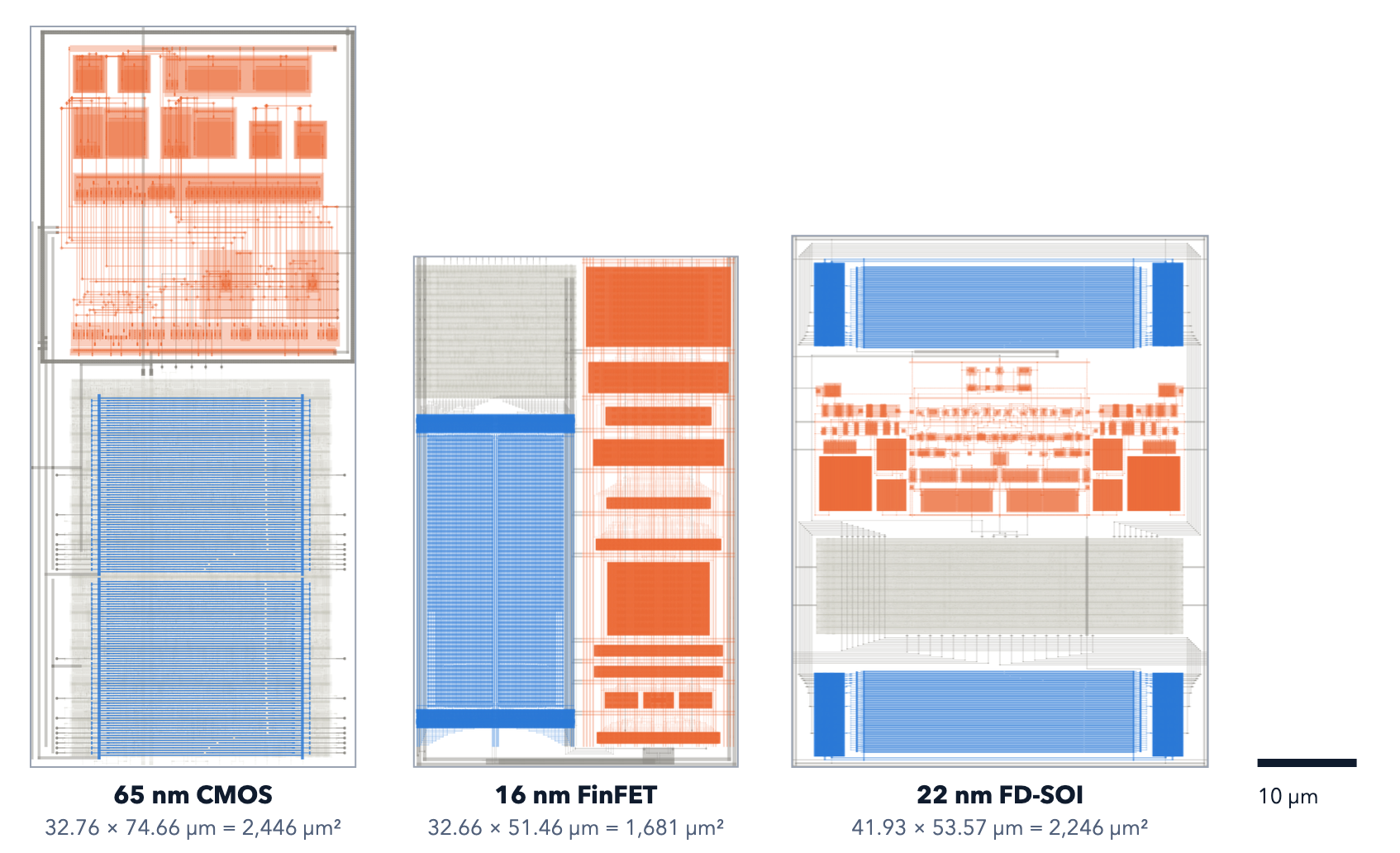
| Macro area (rounded) | 2,400 µm² | 1,700 µm² | 2,200 µm² |
| Power at 5 MS/s | 46.4 µW | 42.4 µW | 25.1 µW |
| Energy / conversion | 9.29 pJ | 8.48 pJ¹ | 5.02 pJ |
| Walden FoM | 11.1 fJ/step | 10.7 fJ/step | 6.4 fJ/step |
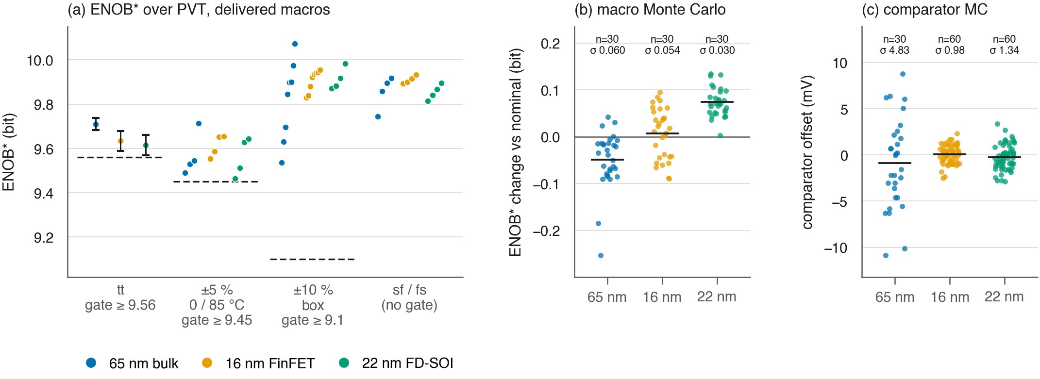
| Lowest ENOB* (±5% supply, 0–85 °C) | 9.491 | 9.555 | 9.464 |
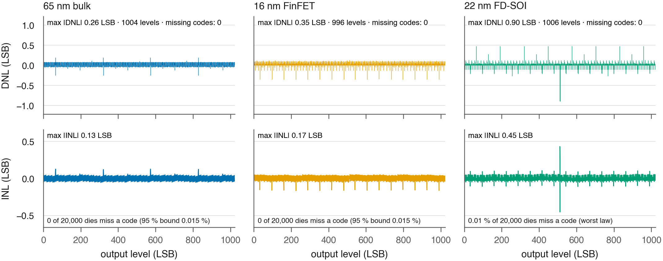
| Missing-code estimate | 0 / 20,000 dies | 0 / 20,000 dies | 0.01% |
| Human hands-on | 4 h 30 (from scratch) | 1 h (port) | 1 h (port) |
*The project’s code-set-corrected metric for short 128-point post-layout records. ¹The 16-nm energy is estimated from a capacitance-only twin record. Monte Carlo missing-code values are estimates, not silicon measurements.
Verification
Block-level evidence and remaining integration gates.
| Check | 65 nm | 16 nm | 22 nm |
|---|---|---|---|
| DRC / LVS / antenna | Recorded | Recorded¹ | Recorded¹ |
| Nominal ENOB* | 9.710 ± 0.028 | 9.634 ± 0.045 | 9.616 ± 0.046 |
| Worst full-accuracy corner | 9.491 | 9.555 | 9.464 |
| Nominal max |DNL| / |INL| | 0.26 / 0.13 LSB | 0.35 / 0.17 LSB | 0.90 / 0.45 LSB |
| Slowest conversion (100 ns window) | 80.8 ns | 87.5 ns | 78.9 ns |
| Start-up words discarded | 10 | 1 | 2 |
¹Multi-patterning deck checks were not run at 16 or 22 nm. The 16-nm electromigration check was not closed because the installed kit lacked limits. The delivered macro packages record these open integration gates; the page does not claim silicon validation.
Architecture & layouts
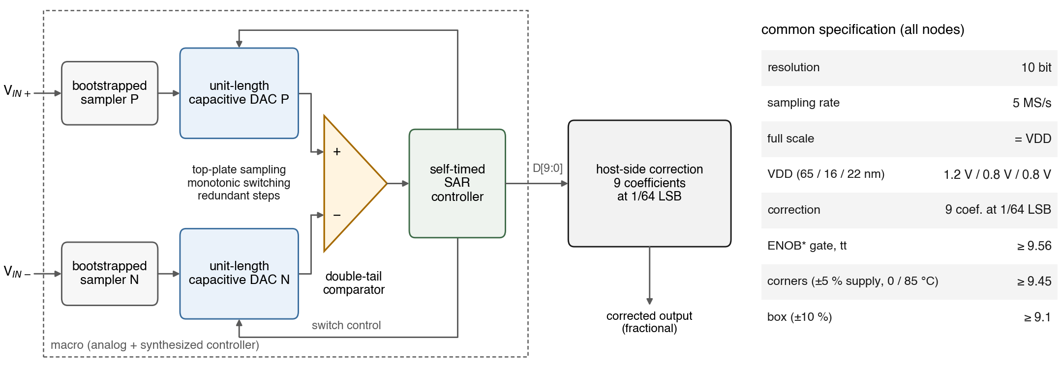
One 10-bit, 5-MS/s specification; three physical implementations.
Survey comparison
Post-layout simulated results alongside measured published ADCs.
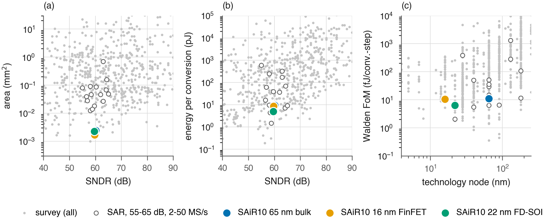
The comparison shows context, not a silicon-to-silicon claim. The same-class subset is identified separately in the source analysis.
Corners & linearity
Accuracy was checked beyond the nominal record.
Output spectra
Typical-corner records with device noise on.
Energy breakdown
Where the conversion energy goes.