
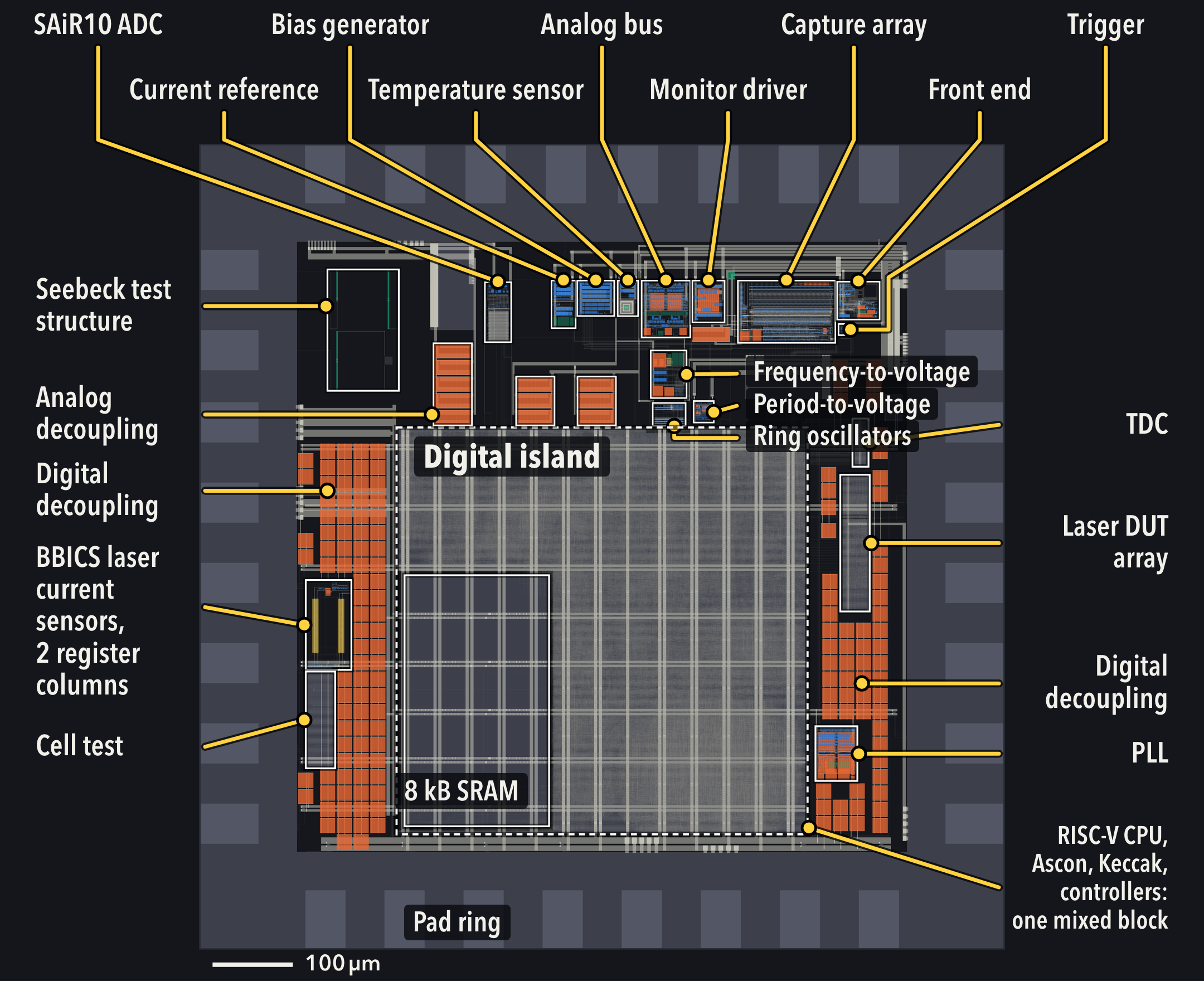
From individual circuits to an integrated chip.
AiSIC brings the circuit portfolio together around a practical research task: applying laser fault injection and observing its effects on the same die. Analog sensors and conversion circuits sit alongside dedicated test structures, a digital processing subsystem and the interfaces needed to control and read the experiment.
| Technology | 65 nm CMOS |
|---|---|
| Die outline | 1 × 1 mm (1 mm²) |
| Integration | 21 blocks: 20 hard blocks and the digital island |
| External connections | 32 pads |
| Digital subsystem | Ibex RV32IMC RISC-V CPU, Ascon-AEAD128, Keccak-f[1600], controllers and 8 kB SRAM |
| Current stage | Post-layout design; fabrication and silicon measurements remain ahead |
The layout rendering shows transistors in blue, resistors in green, capacitors in orange, supply wiring and taps in light grey, and signal wiring in grey. Foundry SRAM, I/O and standard cells appear as plain boxes.
AI execution. Human engineering direction.
The project reports that locally trained AI agents designed the analog blocks and test structures, then carried out chip assembly, placement, routing and checks under human direction. Engineers guided the work, reviewed the results and made design decisions.
One month
Reported elapsed development from the initial idea to the current integrated layout.
~3 business days
Reported total human involvement across the project.
~1 hour per block
Reported approximate human involvement at block level.
These are approximate, project-reported figures from the October 2026 development notes. Human involvement and elapsed development are different measures: hands-on time excludes autonomous execution. The figures are not an independently audited speed-up comparison or a delivery guarantee for another design.
The integrated chip also reuses established digital cores and foundry components, detailed below. The development timeline does not mean every component was created from scratch.
Design, sense, convert and capture.
The analog band combines the SAiR10 SAR ADC, current reference, bias generator and temperature sensor. An analog bus routes internal signals to the ADC and to the external monitor path.
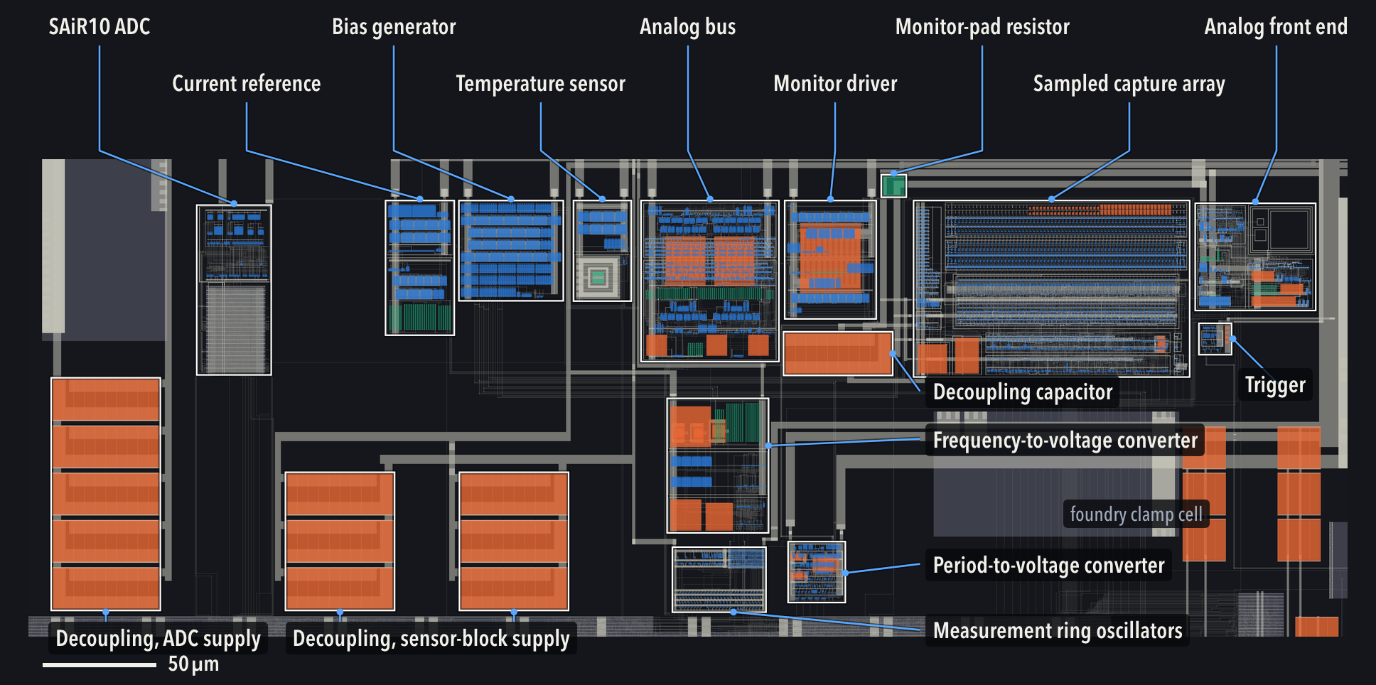
The analog front end converts laser-sensing junction photocurrent to a voltage for the sampled capture array. The frequency-to-voltage and period-to-voltage converters provide complementary readouts of the measurement ring oscillators. A monitor driver exposes selected analog signals at a pad.
Each linked circuit study describes its own simulation conditions and verification limits. Integrating those blocks does not replace the remaining full-chip checks or future silicon measurements.
Built to observe fault injection.
Two register columns, each containing eight flops, sit in separate N-wells watched by built-in current sensors (BBICS). The arrangement lets two sensor designs be compared under laser stimulation. A detected well-current event sets a flag for readout.
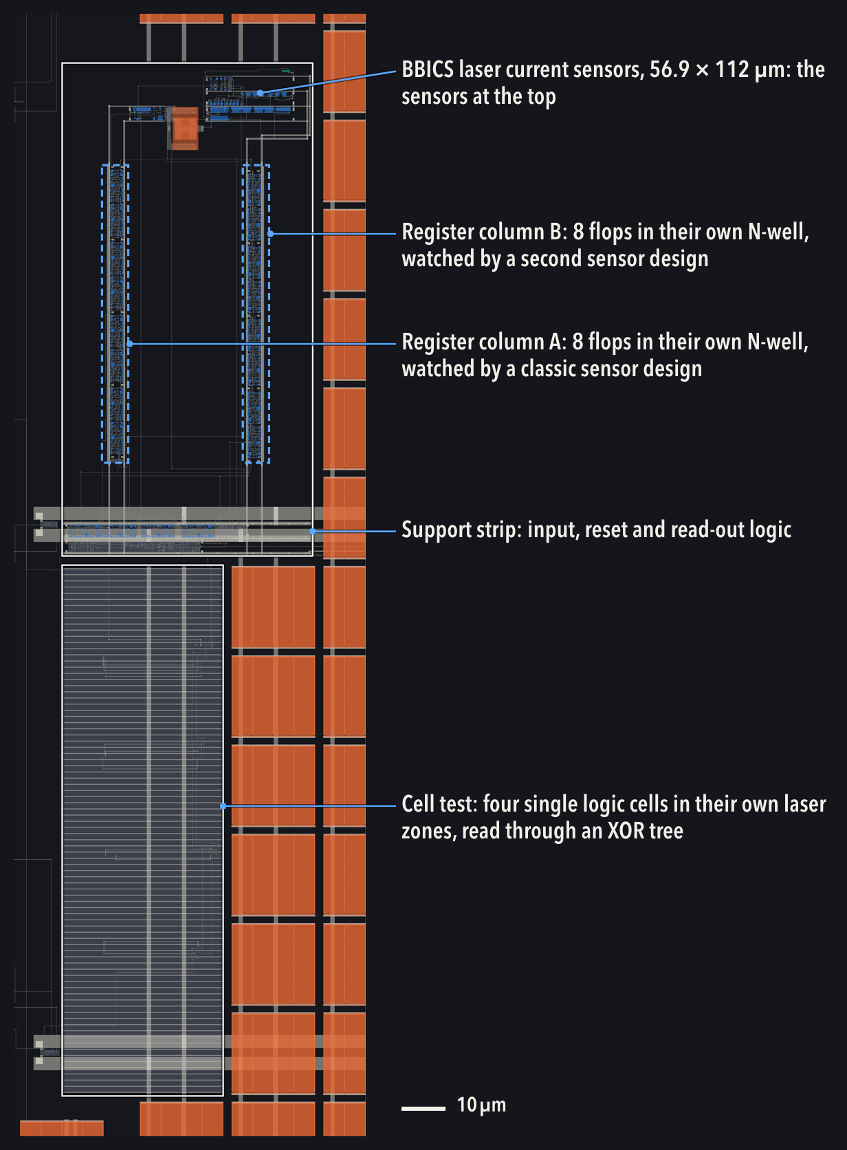
The chip also includes a 16-site logic-chain DUT array, four individual logic-cell test zones, a cell-delay time-to-digital converter and a passive Seebeck test structure for thermal laser stimulation. Together they support experiments on several mechanisms within one integrated platform.
A digital subsystem around the experiment.
The digital island combines an Ibex RV32IMC RISC-V CPU, Ascon-AEAD128 and Keccak-f[1600] with SPI host access, test-structure controllers and an ADC recorder. An 8 kB SRAM provides local storage.
| Component | Origin and role |
|---|---|
| Ibex RISC-V CPU | Unmodified open-source lowRISC core; RV32IMC processing |
| Ascon-AEAD128 | Unmodified open-source Ascon core; cryptographic workload |
| Keccak-f[1600] | Unmodified OpenTitan permutation core; cryptographic workload |
| 8 kB SRAM | Compiled foundry memory |
| I/O and standard cells | Foundry library components |
The AI-assisted contribution covers custom circuit development and chip integration around these existing components. The source notes report the digital island as placed and routed, with static timing met at six corners; silicon operation remains to be validated.
Verification status and remaining work.
The October 2026 project notes report full-chip layout-versus-schematic (LVS) as correct and a verification summary of 19 passed checks, 0 failed checks and 5 provider-dependent checks still open. The remaining work includes foundry cell views and provider reviews. Design-rule exceptions associated with those library views remain unresolved in the reported full-chip state.
Some constituent blocks have accepted verification exceptions, described in their individual studies. The full-chip summary is reported project status, not a fresh verification run performed for this website. It does not establish completed sign-off, a submitted tape-out or measured silicon performance.
A 16-nm FinFET port is a planned next step. It is not presented here as an implemented or verified version of AiSIC.