
From 180 nm to 65 nm CMOS
A held output voltage proportional to clock period, with selectable gain and an output buffer for the pad.
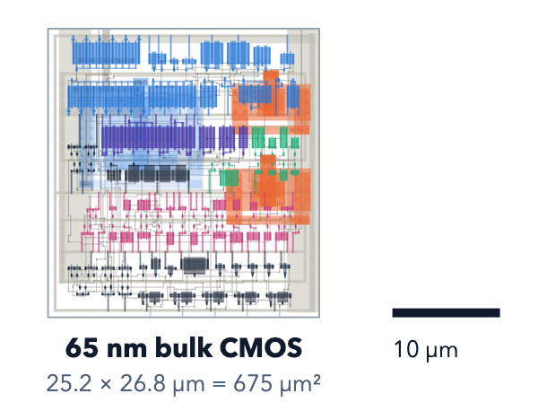
675 µm²
Drawn macro area · 25.2 × 26.8 µm · 65-nm bulk CMOS.
2-bit gain
Gain settings centre the converter at 500 MHz or 1 GHz.
< 1 h hands-on
Human-directed design, layout and verification by AI agents.
Post-layout simulation with extracted parasitics, not silicon measurements.
Charge. Transfer. Reset.
The held voltage is proportional to the clock period.
Charge
While the clock is high, a current charges a capacitor.
Transfer
A transfer pulse shares that charge onto a hold capacitor.
Reset
A reset pulse empties the first capacitor for the next cycle.
Technology migration and added functions
The circuit originates from the SMACD 2026 paper by Santana et al., On-Chip Frequency-to-Voltage Conversion for Hardware Security Characterization. AI agents migrated the design from 180 nm to 65 nm CMOS, added a 2-bit gain code centring it at 500 MHz or 1 GHz, and added an output buffer for the pad.
Human-directed implementation
AI agents performed the design, layout and verification under human direction, with less than one hour of human hands-on time for the work presented here.
The signed-off layout
65-nm bulk CMOS · 25.2 × 26.8 µm · 675 µm²