
What it does
65 nm bulk CMOS · AiSIC SoC
Capture first, read slowly later. The capture array samples the front end's output in two modes. In equivalent-time mode one cell (20 fF) is strobed at a programmable delay, 0 to 7.15 ns in 50-ps steps, one value per repeated laser shot. In single-shot mode 61 cells (5 fF each) are strobed by the taps of one delay line, 20 × 50 ps, then 20 × 100 ps, then 20 × 200 ps (0 to 7 ns), all from one event. The held values are then read out one at a time through a follower in each cell, at about 1 µs per cell (61 µs in total). A dark capture (no laser) with the same timing gives each cell's pedestal and droop.
How it works
65 nm bulk CMOS · AiSIC SoC
The timebase is a line of 60 current-starved inverter units. The 100-ps and 200-ps sections are the 50-ps unit with added MOS-capacitor load, so the section ratio is a capacitance ratio: it drifts 2 to 7 % over process, supply and temperature, against 13 to 21 % for scaled transistor widths. A 7-bit current DAC trims the line delay; for the trim the line closes into a ring oscillator whose period the chip counts, and each tap time is the drawn tap table times the measured line delay. A latch set by the first trigger edge launches the line and keeps every tap in hold through the read-out; a second trigger edge only sets an overflow flag. The single-shot cells use a plain switch without a dummy device, because a dummy's gate leakage dominated the droop.
The layout, at one scale
65 nm bulk CMOS · AiSIC SoC
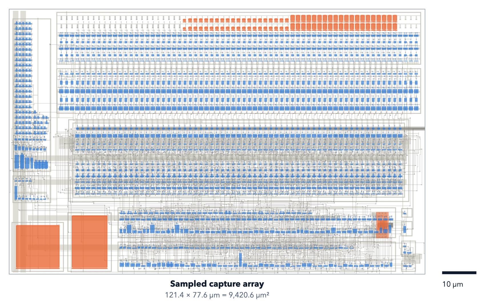
Area (drawn macro outline): Sampled capture array 121.4 × 77.6 µm = 9,420.6 µm².
Key numbers
65 nm bulk CMOS · AiSIC SoC
Post-layout simulation with extracted parasitics, not silicon. 65 nm bulk CMOS. Corners: tt typical, ss / ff slow / fast, sf / fs mixed; temperatures 0 to 85 °C.
| Measure | Value | Specification | Basis |
|---|---|---|---|
| Single-shot waveform error, one common delay offset removed | 1.105–1.752 % | ≤ 2 % of full scale, rms | post-layout, 45 points, each at its trim code |
| Timebase error per tap (tap table + ring count + 3σ mismatch) | 28.3 ps (tt, 27 °C), 41.4 ps (ss, 0 °C), 58.7 ps (ss, 85 °C) | ≤ 100 ps | post-layout, 3 points |
| Equivalent-time mode: edge position after recentring | −7.61 % worst (fast corner) | within 10 % | post-layout, 3 points |
| Droop of the single-shot cells over 62 µs | 0.185 mV (tt, 27 °C), 0.497 mV (tt, 85 °C) | about 1 mV at tt | post-layout |
| Read-out settling to 0.1 mV | 70 ns (tt, 27 °C) to 322 ns (ff, 85 °C) | ≤ 1 µs | post-layout |
| Change of the held values after a second trigger edge | ≤ 0.066 mV | ≤ 1 mV | post-layout, 45 points |
| Hold capacitors as built (61 cells) | −4.68 … −0.68 % of 5.918 fF; 61 of 61 inside | within 5 % | extracted layout, typical corner |
| Gate-oxide overvoltage (above 1.32 V for 0.1 ns or more) | 0 events | 0 events | post-layout, 9 test benches × 15 top-supply points |
| Supply drop | 4.65 mV worst | ≤ 1 % of the supply | post-layout, 5 corners |