
Results at a glance
A 25–100 MHz clock becomes a DC voltage for live monitoring of laser-induced frequency shifts.
| Measure | 65 nm bulk CMOS | 22 nm FD-SOI | 16 nm FinFET |
|---|---|---|---|
| Drawn macro area | 2,639 µm² | 3,625 µm² | 2,265 µm² |
| Frequency resolution, rms¹ | 0.081% | 0.082% | 0.170% |
| Settling, +1% frequency step² | 2.3 µs | 2.6 µs | 3.3 µs |
| Typical power at 50 MHz³ | 32.4 µW | 19.4 µW | 18.5 µW |
¹ Output noise from 10 kHz to 1 MHz, including the on-chip bias reference, divided by the worst sensitivity across the evaluated corners. The 65-nm resolution is schematic-based; the other reported results are post-layout. Resolution targets: 0.1% for 65 / 22 nm, 0.2% for 16 nm.
² Settling to 10% of the applied step; all three settle within 10 µs of switch-on. ³ Excludes the 10-µA bias current. Results are simulations, not silicon measurements.
From clock to voltage
A switched-capacitor charge pump, four gain settings and two RC filters.
Charge
Each clock period, a small capacitor is charged to a reference voltage.
Transfer
The capacitor dumps its charge into a resistor-loaded node. More clock cycles produce a higher output voltage.
Filter
Two RC filters smooth the output. Four gain settings select the pump capacitance.
The hardware-security use case
A ring oscillator changes frequency when illuminated by a laser. Its clock, divided by 16 to 25–100 MHz, feeds this block so the lab can watch a live voltage on an oscilloscope. The chip’s 24-bit counter remains the precise frequency measurement and calibrates the voltage for each chip.
In the 16-nm implementation, flicker noise from the bias reference sets the resolution floor.
Human-directed implementation
AI agents performed the design, layout and verification under human direction, with less than one hour of human hands-on time across the work presented here.
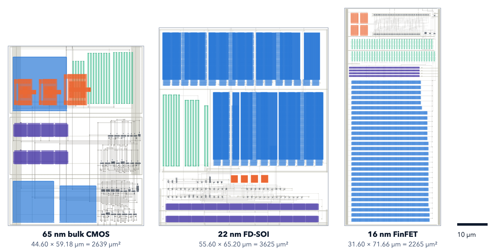
The layouts, at one scale
65-nm bulk CMOS · 22-nm FD-SOI · 16-nm FinFET
Transfer & sensitivity · 65 nm
Schematic and extracted-layout comparison across gain codes and clock frequencies.
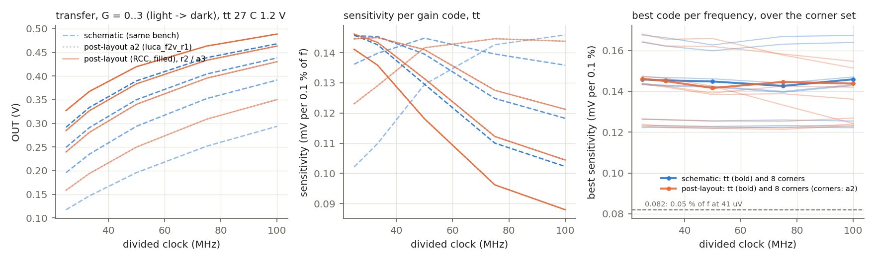
Choose the gain code for the operating frequency, then calibrate the voltage against the counter. The reference and noise basis printed in this earlier figure is not the updated real-bias-chain resolution reported in the overview.
Step response · 65 nm
A +1% step from 50 to 50.5 MHz, gain code 2.
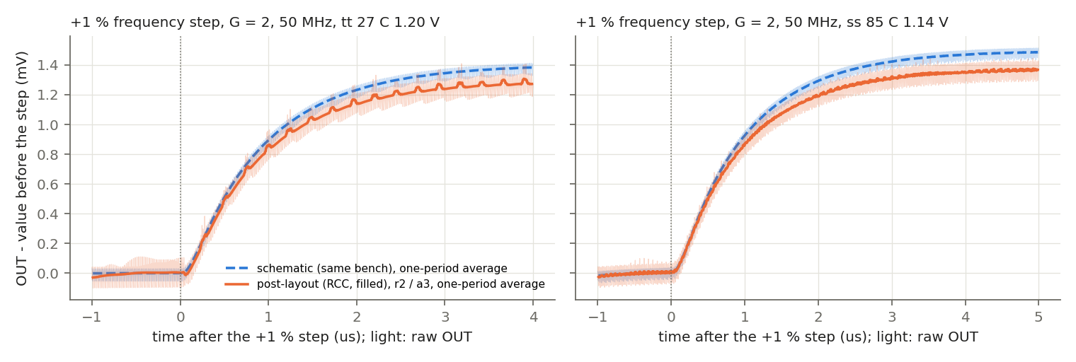
For released r3, the clock-period-averaged output settles to 10% of the step in 2.16 µs at typical conditions and 2.26 µs at the slow condition above. The slower result rounds to the 2.3-µs summary value.