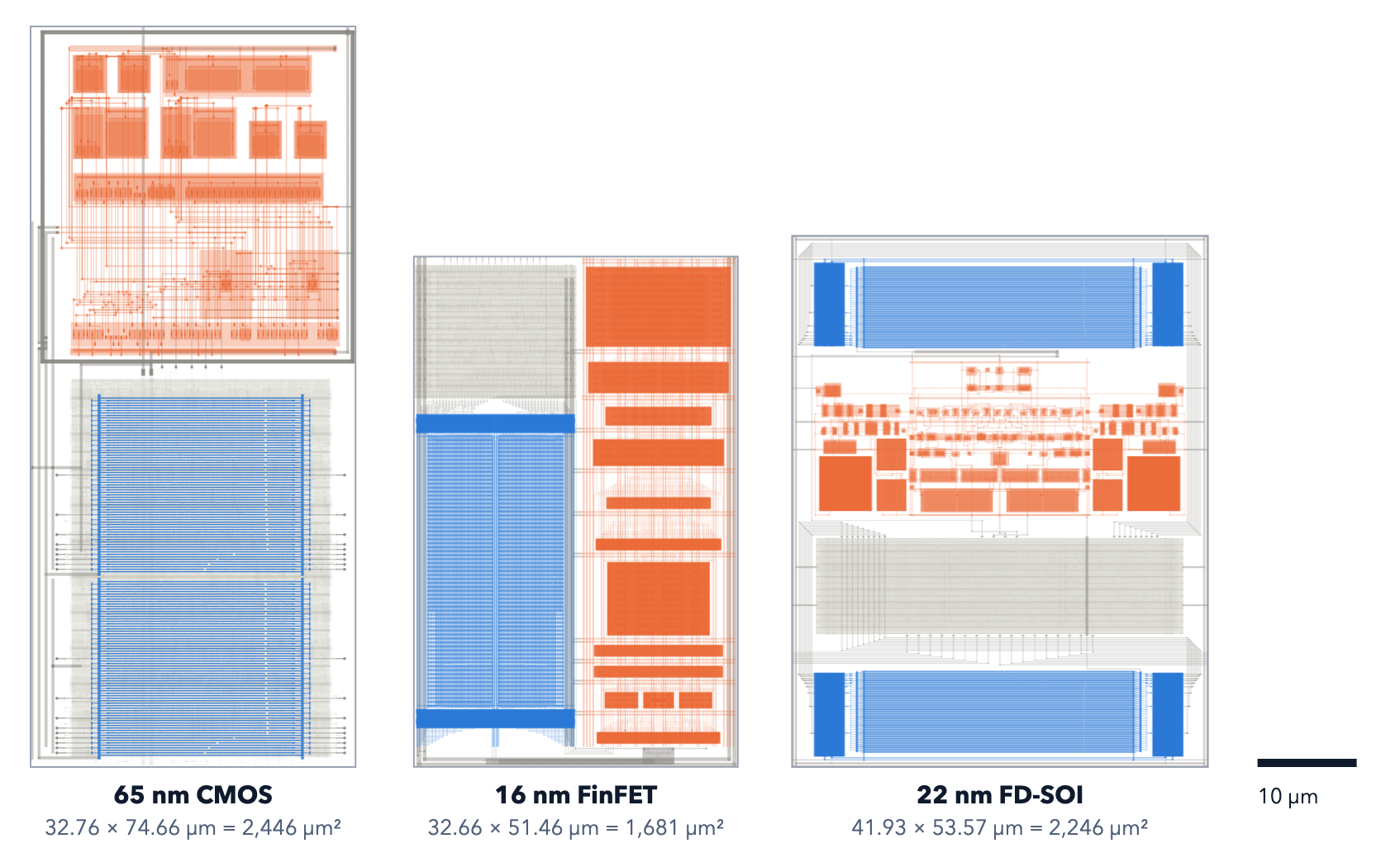
DATA CONVERSION
One ADC. Three technologies.
A 10-bit, 5-MS/s asynchronous SAR ADC developed from a common specification across bulk CMOS, FD-SOI and FinFET.
Layout & extracted-simulation case study

DESIGN SERVICES & IP
Our AI-driven methodology accelerates circuit exploration, simulation and optimization. Experienced engineers guide the process, validate the results, and remain responsible for design decisions and sign-off.
Analog, digital and mixed-signal design shaped around your specifications and integration constraints.
Physical implementation connected to electrical intent, with the checks needed for the agreed design scope.
Move a design towards a new target technology, supply range or application through explicit redesign and comparison.
A DELIVERABLE YOU CAN WORK WITH
Each engagement starts with a concrete engineering objective. We define what will be delivered, how it will be checked, and which decisions remain with your team.
Scope a design projectAgreed schematic, RTL, layout and model views for your environment.
Test conditions, result summaries and the scope of completed checks.
Interfaces, assumptions, operating limits and supporting documentation.
ENGAGEMENT OPTIONS
Evaluate a block, a migration or a difficult design constraint. Leave with a practical scope and the next engineering decisions.
Work towards an agreed set of milestones, design assets and verification deliverables.
Add specialist design and workflow support as your requirements and programme evolve.
FROM THE PORTFOLIO
DATA CONVERSION
A 10-bit, 5-MS/s asynchronous SAR ADC developed from a common specification across bulk CMOS, FD-SOI and FinFET.
Layout & extracted-simulation case study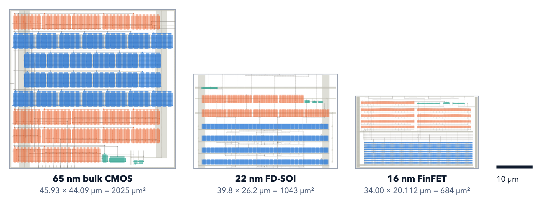
ANALOG BUILDING BLOCK
An eight-output bias generator distributing matched 10-µA currents, adapted and characterized for three process technologies.
Layout & simulation case studyLET’S MAKE IT CONCRETE
Tell us what the circuit needs to do, and where you are starting.